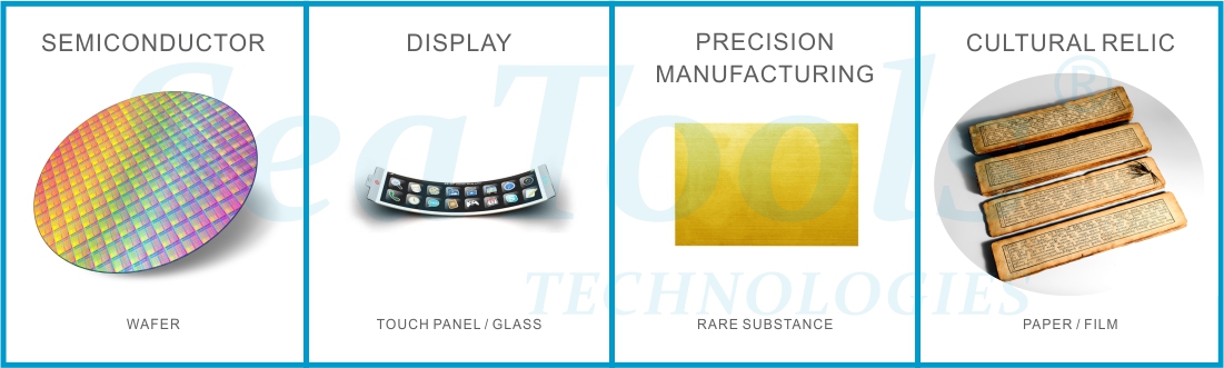
薄片临时键合装备

临时键合是为薄晶圆或待减薄晶圆提供机械支撑的重要工艺,对3D IC、功率器件和FoWLP晶圆以及处理化合物半导体等易碎基板是非常重要的一环。借助于静电夹持力,薄晶片将粘合在薄静电卡盘上,从而允许用薄静电卡盘支撑来处理典型的易碎器晶片。在完成关键工艺之后,薄晶片将被接除键合。

Thin Wafer Temporary bonding is an essential process to offer mechanical support for thin or to-be-thinned wafers, important for 3D ICs, power devices and FoWLP wafers, as well as for handling fragile substrates like compound semiconductors. A device wafer is bonded to a thin e-chuck with the help of temporary bonding with electrostatic clamping force, allowing the typically fragile device wafer to be processed with thin electrostatic chuck support. After the critical processes, the wafer stack is debonded.
特征 | Features

半永久吸附 | 操作便捷 | 校正补平 | 开放式夹持平台
Semi Permanent Adsorption | Convenient Operation | Correction & Leveling | Open Clamp Platform

运用 | Applications

翘曲薄片水平校正 | 易碎薄片补强
Thin wafer horizontal correction | Fragile thin reinforcement

设计及制造 | Design and Manufacture

提供轻柔、翘曲、易碎薄片在进行移载或自动化加工过程中提供半永久吸附,以保证薄片水平状态结构强度,减低自动化加工时夹持碎片风险。
Provide soft, warped and fragile thin, and provide semi permanent adsorption during transfer or automatic processing, so as to ensure the structural strength of thin in horizontal state and reduce the risk of clamping fragments during automatic processing.

核心技术 | Core Technology

Further Product Information

  • Specifications
  • Applications
  • Business
  • Theory
  • Operational Videos